Характеристики
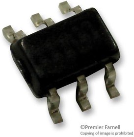
SN74LVC2G06DBVR, ЛН3The SN74LVC2G06DBVR is a dual inverter Buffer/Driver designed for 1.65 to 5.5V VCC operation. The output of this device is an open-drain which can be connected to other open-drain outputs to implement active-low, wired-OR or active-high wired-AND functions. The maximum sink current is 32mA. This device is fully specified for partial-power-down applications using IOFF. The IOFF circuitry disables the outputs, preventing damaging current backflow through the device when it is powered down.
• IOFF Supports live insertion, partial-power-down mode and back-drive protection
• Supports down-translation
• Inputs and open-drain outputs accept voltages up to 5.5V
• Latch-up performance exceeds 250mA per JESD 17
• 3.4ns at 3.3V Propagation delay (tpd)
• 10µA ICC Low power consumption
• ±24mA Output drive at 3.3 V
• 2V at VCC = 3.3V, TA = 25°C VOHV (output VOH undershoot)
• Green product and no Sb/Br
Микросхемы / Логические микросхемы / Микросхемы ТТЛ (серия 74)
Корпус: SOT-23-6, инфо: Двойной буфер-инвертор / драйвер с открытым стоком, примечание: ЛН3
 Личный кабинет


 Загрузка