Характеристики
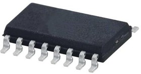
SN74HC367D, ЛП11The SN74HC367D is a Hex Buffer/Line Driver designed specifically to improve both the performance and density of 3-state memory address drivers, clock drivers and bus-oriented receivers and transmitters. The HC367 device is organized as dual 4-line and 2-line buffers/drivers with active-low output-enable (1OE and 2OE) inputs. When OE is low, the device passes non-inverted data from the A inputs to the Y outputs. When OE is high, the outputs are in the high-impedance state.
• True outputs
• High-current 3-state outputs drive bus lines buffer memory address register/drive to 15 LSTTL loads
• 80µA maximum ICC low power consumption
• 10ns typical Propagation delay (tpd)
• ±6mA Output drive at 5V
• 1µA maximum Low input current
• Green product and no Sb/Br
Микросхемы / Логические микросхемы / Микросхемы ТТЛ (серия 74)
Корпус: 16-SOIC N, инфо: Логический элемент ТТЛ Шинный формирователь неинвертирующий 4 х 2 бит КМОП кристалл, примечание: ЛП11
 Личный кабинет


 Загрузка